BAV99WT1, SBAV99WT1G, BAV99RWT1, SBAV99RWT1G�
� http://onsemi.com�
� 4�
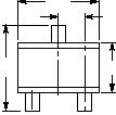
� PACKAGE DIMENSIONS�
� SC?70 (SOT?323)�
� CASE 419?04�
� ISSUE N�
� A�
� A2�
� D�
� e1�
� b�
� e�
� E�
� A1�
� c�
� L�
� 3�
� 12�
� NOTES:�
� 1. DIMENSIONING AND TOLERANCING PER ANSI Y14.5M, 1982.�
� 2. CONTROLLING DIMENSION: INCH.�
� 0.05 (0.002)�
� 1.9�
� 0.075�
� 0.65�
� 0.025�
� 0.65�
� 0.025�
� 0.9�
� 0.035�
� 0.7�
� 0.028�
� SCALE 10:1�
� �
� mm�
� inches�
� *For additional information on our Pb?Free strategy and soldering�
� details, please download the ON Semiconductor Soldering and�
� Mounting Techniques Reference Manual, SOLDERRM/D.�
� SOLDERING FOOTPRINT*�
� HE�
� DIM�
� A�
� MIN NOM MAX MIN�
� MILLIMETERS�
� 0.80 0.90 1.00 0.032�
� INCHES�
� A1�
� 0.00 0.05 0.10 0.000�
� A2�
� 0.70 REF�
� b�
� 0.30 0.35 0.40 0.012�
� c�
� 0.10 0.18 0.25 0.004�
� D�
� 1.80 2.10 2.20 0.071�
� E�
� 1.15 1.24 1.35 0.045�
� e�
� 1.20 1.30 1.40 0.047�
� 0.035 0.040�
� 0.002 0.004�
� 0.014 0.016�
� 0.007 0.010�
� 0.083 0.087�
� 0.049 0.053�
� 0.051 0.055�
� NOM MAX�
� L�
� 2.00 2.10 2.40 0.079�
� 0.083 0.095�
� HE�
� e1�
� 0.65 BSC�
� 0.20 0.560.38�
� 0.028 REF�
� 0.026 BSC�
� 0.015�
� 0.008�
� 0.022�
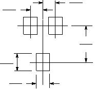
� STYLE 9:�
� PIN 1. ANODE�
� 2. CATHODE�
� 3. CATHODE-ANODE�
� STYLE 10:�
� PIN 1. CATHODE�
� 2. ANODE�
� 3. ANODE-CATHODE�
� ON Semiconductor�
� and are registered trademarks of Semiconductor Co�
� mponents Industries, LLC (SCILLC). SCILLC owns the rights to a number of patents, trademarks,�
� copyrights, trade secrets, and other intellectual property. A listing of SCILLC’s product/patent coverage may be accessed at www.onsemi.com/site/pdf/Patent?Marking.pdf. SCILLC�
� reserves the right to make changes without further notice to any products herein. SCILLC makes no warranty, representation or guarantee regarding the suitability of its products for any�
� particular purpose, nor does SCILLC assume any liability arising out of the application or use of any product or circuit, and specifically disclaims any and all liability, including without�
� limitation special, consequential or incidental damages. “Typical” parameters which may be provided in SCILLC data sheets and/or specifications can and do vary in different applications�
� and actual performance may vary over time. All operating parameters, including “Typicals” must be validated for each customer application by customer’s technical experts. SCILLC�
� does not convey any license under its patent rights nor the rights of others. SCILLC products are not designed, intended, or authorized for use as components in systems intended for�
� surgical implant into the body, or other applications intended to support or sustain life, or for any other application in which the failure of the SCILLC product could create a situation where�
� personal injury or death may occur. Should Buyer purchase or use SCILLC products for any such unintended or unauthorized application, Buyer shall indemnify and hold SCILLC and�
� its officers, employees, subsidiaries, affiliates, and distributors harmless against all claims, costs, damages, and expenses, and reasonable attorney fees arising out of, directly or indirectly,�
� any claim of personal injury or death associated with such unintended or unauthorized use, even if such claim alleges that SCILLC was negligent regarding the design or manufacture�
� of the part. SCILLC is an Equal Opportunity/Affirmative Action Employer. This literature is subject to all applicable copyright laws and is not for resale in any manner.�
� PUBLICATION ORDERING INFORMATION�
� N. American Technical Support: 800?282?9855 Toll Free�
� USA/Canada�
� Europe, Middle East and Africa Technical Support:�
� Phone: 421 33 790 2910�
� Japan Customer Focus Center�
� Phone: 81?3?5817?1050�
� BAV99WT1/D�
� LITERATURE FULFILLMENT:�
� Literature Distribution Center for ON Semiconductor�
� P.O. Box 5163, Denver, Colorado 80217 USA�
� Phone: 303?675?2175 or 800?344?3860 Toll Free USA/Canada�
� Fax: 303?675?2176 or 800?344?3867�
� Toll Free USA/Canada�
� Email: orderlit@onsemi.com�
� ON Semiconductor Website: www.onsemi.com�
� Order Literature: http://www.onsemi.com/orderlit�
� For additional information, please contact your local�
� Sales Representative�
�  �
�
� � �  �
�
� � �  �
�
� � �  �
�
� � �  �
�
� � �  �
�
� � �  �
�
� �  �
�
� � �  �
�
� �  �
�
� �  �
�
� �  �
�
� � �  �
�
� � �  �
�
� � �  �
�
� � 发布紧急采购,3分钟左右您将得到回复。
相关PDF资料
BAV99T116
DIODE SWITCH HI SPEED SOT-23 TR
BAV99TA
DIODE HI SPEED SW DUAL SOT23-3
BAV99W-7
DIODE DUAL SW 75V 200MW SC70-3
BAV99WT1G
DIODE SWITCH SS DUAL 70V SOT323
BAV99
DIODE ULTRAFAST HI CIND SOT-23
BAW101-7
DIODE ARRAY 300V 250MA SOT143
BAW101S,115
DIODE DUAL 300V 250MA SOT-363
BAW101S-7
DIODE ARRAY 300V 250MA SOT363
相关代理商/技术参数
BAV99S
功能描述:二极管 - 通用,功率,开关 1500W 20V 5% UNI TRANSZORB-TVS RoHS:否 制造商:STMicroelectronics 产品:Switching Diodes 峰值反向电压:600 V 正向连续电流:200 A 最大浪涌电流:800 A 配置: 恢复时间:2000 ns 正向电压下降:1.25 V 最大反向漏泄电流:300 uA 最大功率耗散: 工作温度范围: 安装风格:SMD/SMT 封装 / 箱体:ISOTOP 封装:Tube
BAV99S /T3
功能描述:二极管 - 通用,功率,开关 DIODE SW TAPE-11 RoHS:否 制造商:STMicroelectronics 产品:Switching Diodes 峰值反向电压:600 V 正向连续电流:200 A 最大浪涌电流:800 A 配置: 恢复时间:2000 ns 正向电压下降:1.25 V 最大反向漏泄电流:300 uA 最大功率耗散: 工作温度范围: 安装风格:SMD/SMT 封装 / 箱体:ISOTOP 封装:Tube
BAV99S _R1 _00001
制造商:PanJit Touch Screens 功能描述:
BAV99S REG
功能描述:DIODE ARRAY GP 85V 150MA SOT363 制造商:taiwan semiconductor corporation 系列:- 包装:带卷(TR) 零件状态:在售 二极管配置:2 对串联 二极管类型:标准 电压 - DC 反向(Vr)(最大值):85V 电流 - 平均整流(Io)(每二极管):150mA 不同 If 时的电压 - 正向(Vf:1.25V @ 150mA 速度:小信号 =< 200mA(Io),任意速度 反向恢复时间(trr):6ns 不同?Vr 时的电流 - 反向漏电流:1μA @ 75V 工作温度 - 结:-55°C ~ 150°C 安装类型:表面贴装 封装/外壳:6-TSSOP,SC-88,SOT-363 供应商器件封装:SOT-363 标准包装:3,000
BAV99S T/R
制造商:NXP Semiconductors 功能描述:Diode Switching 100V 0.2A 6-Pin TSSOP T/R
BAV99S,115
功能描述:二极管 - 通用,功率,开关 85V 200mA RoHS:否 制造商:STMicroelectronics 产品:Switching Diodes 峰值反向电压:600 V 正向连续电流:200 A 最大浪涌电流:800 A 配置: 恢复时间:2000 ns 正向电压下降:1.25 V 最大反向漏泄电流:300 uA 最大功率耗散: 工作温度范围: 安装风格:SMD/SMT 封装 / 箱体:ISOTOP 封装:Tube
BAV99S,135
功能描述:二极管 - 通用,功率,开关 DIODE SW TAPE-11 RoHS:否 制造商:STMicroelectronics 产品:Switching Diodes 峰值反向电压:600 V 正向连续电流:200 A 最大浪涌电流:800 A 配置: 恢复时间:2000 ns 正向电压下降:1.25 V 最大反向漏泄电流:300 uA 最大功率耗散: 工作温度范围: 安装风格:SMD/SMT 封装 / 箱体:ISOTOP 封装:Tube
BAV99S
制造商:Infineon Technologies AG 功能描述:DIODE DUAL PAIR SOT-363